Samsung presented a new 3D memory architecture at the Future of Memory and Storage (FMS) 2026 conference in Santa Clara that stacks high-bandwidth memory directly above AI accelerators rather than alongside them, while also introducing the industry's first NAND product to exceed 400 layers.
The architecture, called zHBM, inverts the physical layout used in current HBM deployments. Where today's packages place the high-bandwidth memory die beside the processor on the same substrate, zHBM bonds memory vertically above the accelerator chip to shorten the distance data must travel between the two. Per Samsung, a system built around zHBM is expected to deliver approximately eight times the performance of HBM5 and more than ten times its memory density, with energy efficiency improving threefold and thermal resistance cut by more than half. An additional design feature allows customer-specific logic to be embedded in the interlayer between the memory and the AI accelerator, letting chipmakers integrate custom silicon between the two without redesigning either die.
Samsung also showed the zNAND-O concept, a next-generation NAND architecture based on its V-NAND technology and intended for edge AI environments. Available in four- and eight-layer configurations, zNAND-O combines high space efficiency and low latency for real-time, data-intensive inference workloads at the edge.
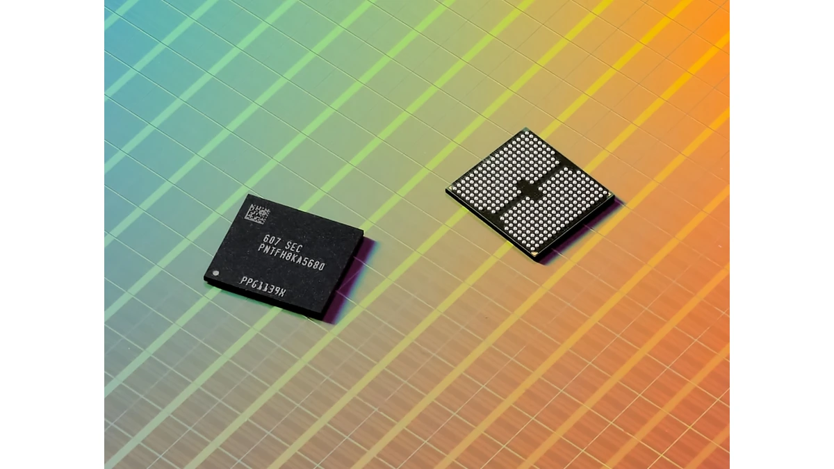
The conference marked the industry debut of Samsung's V10 BV-NAND, the company's tenth-generation 3D NAND product and the first to exceed 400 layers. Samsung reached that milestone by applying wafer bonding technology to stack memory cells, a process that lifts storage density by approximately 58% over the previous V9 generation. Read, write, and I/O performance improve alongside the density gain. Samsung introduced the original V-NAND architecture in 2013; the V10 is the first generation to use wafer bonding as the primary stacking method.
Alongside its roadmap concepts, Samsung featured its current shipping portfolio at FMS. HBM4E, for which Samsung began shipping samples to global customers in May, was on display together with HBM5 and LPDDR5X-PIM, described as the first LPDDR memory with processing-in-memory capability built in. Enterprise storage options PM1763 and BM1773 rounded out the booth. Samsung framed the full lineup as a one-stop strategy: as the only integrated device manufacturer (IDM) that designs and manufactures memory, foundry logic, and advanced packaging in-house, Samsung says it can shorten development cycles for customers building custom AI silicon.
The practical question left open by the FMS presentation is when zHBM reaches production. The architecture remains a concept model and Samsung gave no ship timeline, but the design direction signals where high-bandwidth memory is heading as AI accelerator makers push to close the growing gap between processor compute throughput and memory bandwidth.