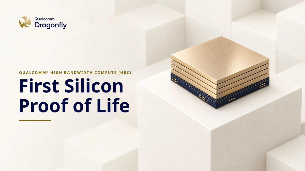
Qualcomm HBC, the compute-near-memory technology planned for the company's next data center inference accelerator, has completed hardware validation in first-generation silicon. Qualcomm says that silicon ran the full memory read-write path and near-memory computations in its San Diego lab on industry-standard automated test equipment.
The test used randomized weights and activations at production-representative dimensions. Qualcomm expresses the gains as bandwidth and efficiency estimates built from measured results, normalized to target operating conditions and compared against competitors' published specifications, and it cautions that final performance may vary by product implementation, workload and system configuration.
The problem Qualcomm HBC targets is data movement. Generating each token means feeding model data to the compute units, and at data center scale the energy and latency of that traffic shape throughput and cost. HBC puts compute closer to the memory to cut the movement. Qualcomm describes wafer-to-wafer bonding developed with foundry and assembly partners, plus redundancy and remapping to work around memory defects. An unnamed data center product has taped out, and early bring-up of a logic base with bonded DRAM tiers is yielding, per Qualcomm.
Qualcomm names the Dragonfly AI250 as the next step: it is expected to sample in the first half of 2027 and will integrate HBC into a complete inference accelerator. Qualcomm places it in a three-step Dragonfly accelerator roadmap:
| Accelerator | What Qualcomm lists |
|---|---|
| Dragonfly AI200 | Rack-scale inference focused on memory capacity and total cost of ownership |
| Dragonfly AI250 | HBC Gen 1; 18x the effective memory bandwidth of AI200 |
| Dragonfly AI300 | Third generation with HBC Gen 2; 54x the effective bandwidth per card versus AI200 |
Both multipliers are measured against Qualcomm's own AI200 and use the company's effective-bandwidth figure. Against rival designs, Qualcomm claims 6x the memory bandwidth per watt of HBM-based systems, an estimate it derives from competitors' published specifications normalized at card level.
Qualcomm specifies the AI250 rack with 56 cards, 43 TB of memory and 7.455 PB/s of effective bandwidth. Each card carries 768 GB and 133 TB/s of effective bandwidth, and the rack has a 140 kW thermal design power. It scales up over PCIe 6.0 and out over Ethernet with RoCE, and it takes either air or direct liquid cooling.