LG Innotek displayed a new class of chip-packaging substrate built for AI accelerator chips for the first time, at KPCA show, an annual PCB and semiconductor-packaging trade show held September 9 through 11 at Songdo Convensia in Incheon, South Korea. The component is an FC-BGA, or flip chip-ball grid array, the layer of circuitry that connects a semiconductor chip to the mainboard beneath it, and this version is built for the extra wiring that dense AI processors require. LG Innotek was among more than 350 companies at the show, now in its 23rd year.
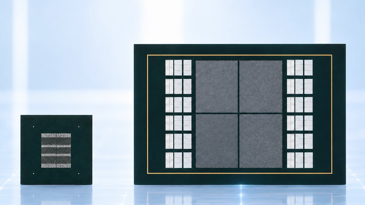
That AI-accelerator FC-BGA measures more than 100 millimeters on a side, large enough to carry the additional circuits and components that graphics processors (GPUs) and neural processing units (NPUs) need compared with general-purpose FC-BGA. LG Innotek said it aims to reach mass production for the part by 2027, building on more than 50 years of substrate work that includes ultra-fine circuitry and high layer counts. The company's booth also carried an 85-by-85-millimeter FC-BGA and an even larger sample substrate with roughly 40% more surface area than that.
Alongside the accelerator substrate, LG Innotek highlighted the packaging technology meant to set it apart from competitors. Chip embedding buries the chip inside the substrate rather than mounting it on the surface, shortening the connection between chip and board to improve signal transmission while lowering the electrical resistance that wastes power. A glass-substrate design, which the company is targeting for mass production by 2028, replaces the substrate's internal core layer with glass to cut down on warping and circuit distortion. A separate copper-pillar method the company calls Cu-Post tightens the spacing between solder balls by about 20% versus earlier designs and relies on copper's higher thermal conductivity than lead to manage heat. LG Innotek also showed ECONOVA, a smart IC substrate it says is the industry's first to reach high performance without palladium or gold plating, a materials change aimed at European environmental rules.
LG Innotek's package-solutions business, which includes the substrate lines on display, posted first-half revenue of ₩935.6 billion (about $692 million) and operating profit of ₩99.6 billion (about $74 million), up 18% and 94% year over year. Operating margin rose from 6.5% to 10.6% over the same period, and the company is targeting ₩1 trillion (about $740 million) in annual operating profit from the business by 2031.
A photo LG Innotek released with the substrate shows the new AI-accelerator FC-BGA next to a PC FC-BGA sample roughly six times smaller, illustrating how much more circuitry the AI-era part has to carry. "This exhibition will let people see intuitively how LG Innotek's substrates are used across AI, smartphones and mobility in everyday life," said Jo Ji-tae, head of LG Innotek's package-solutions business, who added that the company intends to lead a shift in the substrate market with its newer designs.