South Korea's government announced an 800 trillion won ($520 billion) public-private semiconductor investment program on Monday, with Samsung Electronics and SK Hynix committing to build four new fabrication plants and dedicated high-bandwidth memory packaging facilities as the country races to cement its lead in the chips powering AI infrastructure.
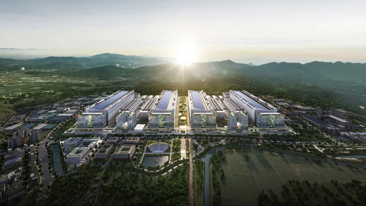
According to Nikkei Asia and Tom's Hardware, South Korean President Lee Jae Myung made the announcement at the Blue House presidential palace in Seoul, joined by Samsung Electronics Chairman Lee Jae-yong and SK Group Chairman Chey Tae-won. The plan calls for Samsung and SK Hynix each to build two new fabs in the southwestern region near Gwangju, an area that has historically sat outside the main semiconductor belt south of Seoul. Samsung will separately construct high-bandwidth memory (HBM) packaging facilities in the Chungcheong region, targeting the Cheonan and Onyang areas specifically.
The investment is structured as a coordinated public-private commitment rather than a direct government spending program. Industry Minister Kim Jung-kwan said the government and industry would jointly invest more than 30 trillion won over 15 years across the semiconductor supply chain, while regional governments in Gwangju and South Jeolla province would contribute 5 trillion to 20 trillion won. An additional 81 trillion won was directed toward the Chungcheong packaging hub. The government did not disclose the exact public-private split on the headline 800 trillion won figure; analysts expect the bulk to be company capital expenditure coordinated under state direction, with Seoul's contribution concentrated in subsidies, faster permitting, and infrastructure.
The permitting acceleration may be the most operationally significant piece. Minister Kim said the plan would shorten the timeline from licensing to operational fab by up to 12 years, pulling completion from the mid-2040s to the mid-2030s. SK Hynix's Yongin memory complex, previously scheduled for mid-decade-next, has been moved up a full 12 years under the revised framework. The stated goal is to double South Korea's total memory output within five years.
The commercial pressure behind the announcement is clear. SK Hynix overtook Samsung as South Korea's most valuable listed company this month, driven by its leading position in HBM supply to Nvidia's AI accelerator line. Samsung's semiconductor division posted 53.7 trillion won in first-quarter operating profit as AI-driven memory shortages are forecast to run past 2027. SK Hynix had separately committed $15 billion to new facilities in February, a figure now absorbed into the larger national framework. The new fabs are aimed directly at the strain point: HBM production capacity, which requires advanced stacking processes equivalent in complexity to front-end logic fabs.
The scale invites a direct comparison with the United States' CHIPS Act, which authorized roughly $52 billion in government subsidies. South Korea's figure is ten times larger, though the comparison is asymmetric: the American number is direct federal subsidy, while most of the Korean total is coordinated private investment backed by state permitting and infrastructure support. Both programs share the same strategic logic: secure domestic capacity for the memory and logic chips that underpin AI workloads at a moment when the US, China, Japan, and the European Union are all pursuing their own semiconductor industrial strategies. For Seoul, the specific target is memory, where Samsung and SK Hynix together hold dominant global share, and the stated goal is to extend that lead.