High-bandwidth memory (HBM) is a stacked DRAM design that sits beside a GPU or AI accelerator inside the same package so the chip can read and write data far faster than board-mounted memory allows. It only works because of advanced packaging, the set of techniques that place several dies side by side or on top of each other. Co-packaged optics applies the same idea to networking, pulling the optical transceiver into the processor package. All three answer one problem: compute keeps getting faster, and moving data to it is now the harder part.
SK hynix puts a number on that gap. In its summary of a Nature Electronics review it co-authored, the company says compute throughput has typically tripled every two years while interconnect bandwidth has grown only about 1.4-fold over the same period, a gap it calls the bandwidth wall. HBM eased the memory bottleneck inside the package; co-packaged optics targets the wall between packages.
How High-Bandwidth Memory Is Built
High-bandwidth memory (HBM) gets its speed from width rather than clock rate. The JEDEC HBM4 standard gives each stack a 2048-bit interface at up to 8 Gb/s per pin, for up to 2 TB/s, and SK hynix, Samsung and Micron all quote faster parts. Stacking DRAM dies and placing them inside the processor package is what makes that width practical.
Micron describes HBM as a 3D-stacked DRAM in which several memory dies sit on an optional base die, joined by thousands of through-silicon vias (TSVs) and microbumps. Micron says a single HBM cube carries a 1024-bit data interface split into 32 independent channels, 16 times wider than a standard DDR5 module. The stack then joins the CPU or GPU in a system-in-package over a silicon interposer, which shortens the distance each bit travels.
From the bottom up, a typical HBM stack has four layers of engineering:
- Silicon interposer or bridge: the wiring layer under both the processor and the memory, dense enough to carry thousands of short connections.
- Base die: the logic die at the bottom of the stack that talks to the processor. Samsung builds its HBM4 base die on a 4nm logic process, borrowed from its foundry side.
- DRAM core dies: the memory layers themselves. The HBM4 standard allows 4-high, 8-high, 12-high and 16-high stacks, the source of the 12-high and 16-high labels on spec sheets.
- Through-silicon via and bonding layers: vertical electrical paths through each die, plus the material that holds the stack together and pulls heat out.
The bonding step is one place the memory makers take different routes. SK hynix uses a process it calls Advanced MR-MUF, which injects a liquid protective material between stacked chips and hardens it; the company says the method dissipates heat better than laying film on each layer, and that its warpage control lets it stack chips 40% thinner than earlier generations. Samsung's HBM documentation instead describes Non-Conductive Film (NCF), an insulating adhesive used with copper microbumps. Both aim at the same problem: stacking more thin dies while keeping the stack flat and cool.
HBM Generations and Who Makes HBM Chips
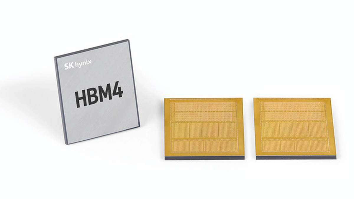
HBM4 is the generation now shipping, and its headline change is a doubled interface. Micron says HBM4 moves to a 2048-pin bus running faster than 11Gbps, for more than 2.8 TB/s of memory bandwidth per stack, against more than 1.2 TB/s per stack for its HBM3E. SK hynix cites a JEDEC baseline of 8Gbps for HBM4 and Samsung an industry standard of 8Gbps, and both say their parts exceed it. Samsung says it began mass production and shipped commercial HBM4 to customers first, and SK hynix says it was first to finish HBM4 development and prepare mass production.
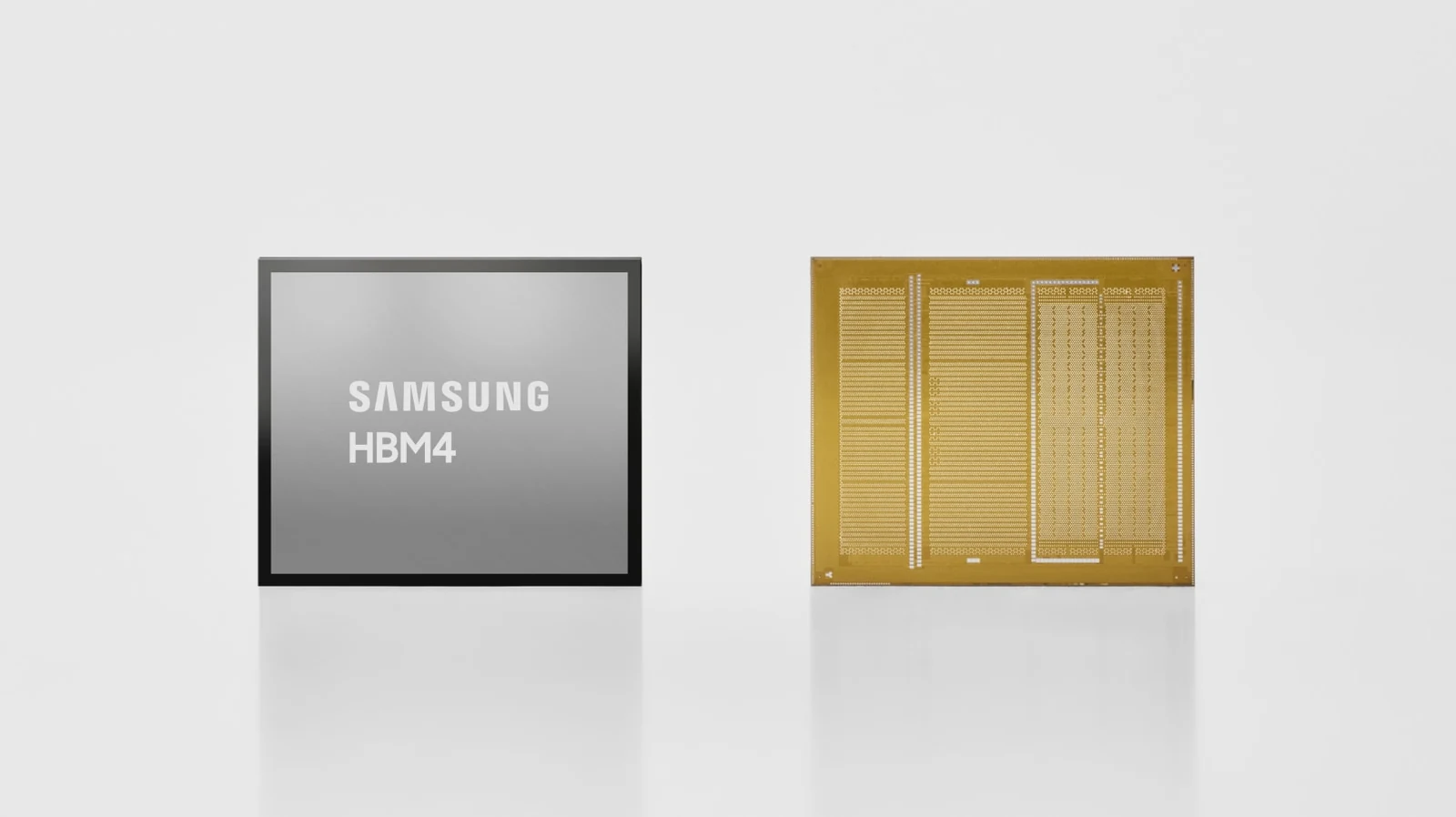
SK hynix, Samsung and Micron each make HBM, and each publishes its own HBM4 specifications. JEDEC published the HBM4 standard, JESD270-4, in April 2025; beyond the wider bus, it doubles the independent channels per stack from 16 in HBM3 to 32 and allows stacks of up to 64GB. Samsung's HBM product pages show how far each generation has moved:
| Generation | Pin speed | Bandwidth per stack | Interface | Stack and capacity |
|---|---|---|---|---|
| Samsung HBM3 | 6.4Gbps | Up to 819 GB/s | 1024-bit | 8-high or 12-high, 16GB or 24GB |
| Samsung HBM3E | Up to 9.2Gbps | Up to 1,180 GB/s | 1024-bit | 8-high or 12-high, 24GB or 36GB |
| HBM4, JEDEC standard | Up to 8Gbps | Up to 2 TB/s | 2048-bit | 4-high to 16-high, up to 64GB |
| Samsung HBM4E | Up to 16Gbps | Up to 4 TB/s | 2048-bit | 16-high, up to 64GB |
The HBM4 parts the three makers have announced differ in speed bin and stack height, so compare them by the figures each one publishes:
| Vendor and part | Pin speed | Bandwidth per stack | Capacity and stack | Process notes |
|---|---|---|---|---|
| Micron HBM4 | Above 11Gbps | Above 2.8 TB/s | 36GB 12-high; 48GB 16-high sampling | 2048-pin interface |
| Samsung HBM4 | 11.7Gbps, up to 13Gbps | Up to 3.3 TB/s | 24GB to 36GB 12-high; up to 48GB 16-high planned | 1c DRAM, 4nm logic base die |
| SK hynix HBM4 | Above 10Gbps | Double the previous generation | N/A | 1b nm DRAM, Advanced MR-MUF |
Power efficiency is the other half of the pitch. Samsung claims a 40% gain in power efficiency over HBM3E from low-voltage through-silicon via design and power-delivery tuning, and SK hynix claims more than 40% for its own HBM4. The more telling detail is the base die. Once it moves to a 4nm logic process, a memory stack becomes partly a foundry product, and Samsung presents the co-optimization between its foundry and memory businesses as an advantage.
At the chip level the stacks add up. NVIDIA says its Rubin GPU carries up to 288GB of HBM4 with aggregate bandwidth of up to 22 TB/s, and that HBM4 doubles the interface width of HBM3E. That per-GPU figure, not the per-stack one, is the number that matters when comparing accelerators.
HBM Against DDR5, GDDR7 and LPDDR5X
High-bandwidth memory (HBM) is DRAM too, so setting it against DDR5 or GDDR7 is a question of how the memory connects rather than what it is made of. Micron puts the split plainly: a standard DDR5 module relies on a narrower bus running at very high clock speeds, while HBM uses a wide, highly parallel interface that Micron says moves data at much lower energy per bit.
| Memory | How it connects | Example from a vendor spec |
|---|---|---|
| HBM | Stacked dies beside the processor in one package | NVIDIA Rubin GPU: up to 288GB of HBM4, up to 22 TB/s |
| GDDR7 | Chips on the circuit board around the GPU | NVIDIA GeForce RTX 5090: 32GB of GDDR7 |
| DDR5 | Modules with a narrower, faster-clocked bus | Micron: one HBM cube is 16 times wider than a standard DDR5 module |
| LPDDR5X | Low-power DRAM paired with CPUs | NVIDIA Grace CPU Superchip: LPDDR5X at up to 1 TB/s |
HBM can also serve as a CPU's main memory. Intel's Xeon CPU Max Series, which Intel lists with a first-quarter 2023 launch date, carries 64GB of HBM2e across four stacks inside the package, and Intel says buyers can eliminate DDR for workloads that fit within 64GB and need 1 to 2GB of memory per core. Two current PC graphics cards show the alternative: NVIDIA's GeForce RTX 5090 ships with 32GB of GDDR7, and AMD lists GDDR6 for the Radeon RX 9070 XT.
Advanced Packaging: Interposers, Bridges and 3D Stacks
Advanced packaging is what lets HBM sit millimeters from the processor at all. Samsung's foundry splits the field into horizontal and vertical integration: chips placed side by side on a shared base, or stacked to shorten wires further, which Samsung says also cuts the yield risk of very large monolithic dies. Intel Foundry's packaging lineup shows the main options in one catalog:
- EMIB 2.5D: a small silicon bridge embedded in the package substrate that links neighboring dies edge to edge, including logic to HBM. Intel says it has been in mass production since 2017, and the EMIB-T variant adds through-silicon vias to the bridge.
- Foveros-S 2.5D: a full silicon interposer of up to four times the reticle size, for designs with several chiplets on top.
- Foveros Direct 3D: chiplets stacked on an active base die through copper-to-copper hybrid bonding, which Intel pitches for high bandwidth and low power between dies.
- EMIB 3.5D: bridges and 3D stacks in one package. Intel says its Data Center GPU Max used it to combine 47 active tiles and more than 100 billion transistors.
Shipping accelerators show what this buys. NVIDIA says every Blackwell product joins two reticle-limited dies with a 10 TB/s chip-to-chip link so they behave as one GPU. AMD's Instinct MI355X pairs its compute with 288GB of HBM3E and 8 TB/s of peak memory bandwidth. Die-to-die links are also getting a common language: Intel says it helps drive interconnect standards such as Universal Chiplet Interconnect Express (UCIe). For the wider role of these parts in AI systems, the comparison of GPU vs TPU vs custom accelerators for AI inference covers how vendors balance compute and memory.
Co-Packaged Optics Moves the Transceiver Into the Package
Co-packaged optics (CPO) carries the advanced packaging idea from memory to the network. Seunghoon Hong, who leads the AI infrastructure team at SK hynix, describes CPO as integrating optical transceivers into the same package as the processor, so chips exchange data using light instead of long electrical traces. Conventional switches use pluggable transceivers, optical modules that plug into the switch's ports; NVIDIA's CPO switches instead put silicon photonics on the same package as the switch ASIC. SK hynix says that moving the optical engine closer to the processor minimizes the distance electrical signals travel, which improves both bandwidth and energy efficiency.
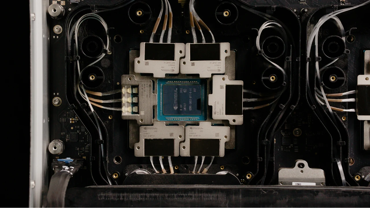
According to SK hynix's summary, the authors of the Nature Electronics review set targets for the next stage: more than 100 Tb/s of bandwidth per node, energy below 1 pJ/bit and chip-to-chip latency under 10 nanoseconds. Its roadmap runs from 2D and 2.5D interposer-based layouts to 3D stacking, and eventually to a photonic interposer that links pools of processors and memory by light. That last step is a research direction, not a product.
Network switches are where co-packaged optics has already reached products, from both NVIDIA and Broadcom.
| Vendor | CPO product | Vendor claim |
|---|---|---|
| NVIDIA | Spectrum-X and Quantum-X Photonics switches | Silicon photonics on the ASIC package replaces pluggable transceivers, with 5x better power efficiency |
| Broadcom | Tomahawk 6-Davisson, its third CPO generation | First 100T CPO Ethernet switch at 200G per lane |
| Broadcom | Tomahawk 5-Bailly, the previous generation | 65% power saving against retimed optics; no link flaps in the first 1 million device hours |
NVIDIA says its Spectrum-X Ethernet Photonics switches have ramped to full production, and it names CoreWeave, Lambda, Meta, Microsoft and Oracle Cloud Infrastructure as first adopters. For an operator working to a fixed power budget, that efficiency claim is the first one worth testing.
Benefits and Trade-Offs
HBM, advanced packaging and co-packaged optics share one benefit, shorter electrical paths, and they share most of their costs too.
Advantages
- Bandwidth density: an HBM4 stack moves terabytes per second in what Micron calls a drastically reduced physical footprint.
- Energy per bit: Micron says HBM's wide interface moves data at much lower energy per bit, and SK hynix says moving optics closer to the processor improves energy efficiency.
- Bigger effective chips: bridges, interposers and hybrid bonding let designers exceed the reticle limit of one die, as Blackwell's two-die design shows.
- Signal integrity: SK hynix says optical links bring strong signal integrity and better immunity to electromagnetic interference than long copper runs.
Limitations
- Heat and power in one spot: Samsung says doubling HBM4 data I/Os from 1,024 to 2,048 pins created power and thermal challenges it had to design around, and AMD rates the MI355X at 1,400W typical board power.
- Capacity set at purchase: HBM ships inside the processor package, as Micron describes it, so treat its capacity as fixed and size it for the workload before buying.
- Yield and assembly risk: every extra die in a package is another part that must be known-good before assembly, which is why Intel Foundry sells die-level sort and burn-in to find known-good die.
- Serviceability: a pluggable transceiver is a separate module, while co-packaged optics ties the optical engine to the switch package. Broadcom's briefing reports no link flaps in the first 1 million CPO device hours, and NVIDIA says its CPO switches need fewer components and are easier to install and replace than pluggable transceivers.
Where HBM and CPO Fit, and Where They Do Not
High-bandwidth memory (HBM) pays off where a processor is starved for data and the budget can absorb it: AI training and inference accelerators, HPC chips and the largest GPUs. Outside that band, cheaper memory often does the job. NVIDIA itself chose 128GB of what it calls cost-efficient GDDR7 for Rubin CPX, a GPU aimed at the context phase of long-prompt inference, and its Vera Rubin platform also pairs HBM-based Rubin GPUs with SRAM-based Groq 3 LPX accelerators for low-latency inference. For desktop graphics cards, the GPU buying guide covers how much VRAM a card actually needs.
CPUs mostly stay with conventional DRAM; even NVIDIA's Vera CPU pairs its cores with LPDDR5X rather than HBM, and the DDR5 vs DDR4 RAM comparison sets out what that tier delivers. Co-packaged optics has an even narrower fit. SK hynix says copper interconnects remain the cost-effective choice over short distances, so short links can stay on copper while CPO targets the longer, faster paths across racks and pods in large AI clusters. For operators sizing those clusters, the explainer on how AI models are served at scale shows where memory and network bandwidth enter the bill.
For buyers of AI hardware, memory and network specs deserve the same scrutiny as compute specs. Two accelerators with similar compute figures can behave very differently if one carries more HBM stacks or faster pins, and NVIDIA and Broadcom both pitch co-packaged optics on lower power than pluggable or retimed optics.
Further reading
Frequently Asked Questions
What is the maximum bandwidth of HBM memory?
Up to 2 TB/s per stack under the JEDEC HBM4 standard, and vendors go further. Samsung lists up to 3.3 TB/s for its HBM4 and up to 4 TB/s for HBM4E. Per chip, the stacks add up. NVIDIA says its Rubin GPU reaches up to 22 TB/s of aggregate HBM4 bandwidth.
Is HBM faster than DDR5?
Per device, yes, because it is far wider. Micron says a single HBM cube has a 1024-bit interface with 32 independent channels, 16 times wider than a standard DDR5 module, which instead runs a narrower bus at very high clock speeds. Both are DRAM. The difference is that HBM stacks its dies beside the processor inside one package, which Micron says also cuts the energy spent per bit.
Why don't PCs use HBM?
PC graphics cards can get by with GDDR memory: NVIDIA's GeForce RTX 5090, for example, ships with 32GB of GDDR7. HBM stacks DRAM dies next to the processor inside one package, while GDDR7 chips sit on the circuit board around it. Even NVIDIA describes the 128GB of GDDR7 on its Rubin CPX data center GPU as cost-efficient memory. HBM also needs advanced packaging: Micron says the stack joins the processor in a system-in-package over a silicon interposer.
Who makes HBM chips?
SK hynix, Samsung and Micron each make HBM and publish HBM4 parts. Samsung says it began mass production and shipped the first commercial HBM4, SK hynix says it was first to finish HBM4 development, and Micron says it is in high-volume production of a 36GB 12-high HBM4 stack. Their speed bins differ, so compare parts by each vendor's published figures.
Can HBM be used as RAM?
Yes, on processors built for it. Intel's Xeon CPU Max Series, an early-2023 product line, carries 64GB of HBM2e in the package across four stacks, and Intel says buyers can eliminate DDR for workloads that fit within 64GB and need 1 to 2GB of memory per core. On accelerators such as AMD's Instinct MI355X, with 288GB of HBM3E, it already is the main memory.
Does co-packaged optics replace copper cables?
Not for short links. SK hynix notes that copper interconnects remain cost-effective over short distances but need more compensation circuitry, power and latency as speed and reach grow. Co-packaged optics targets those longer, faster links across racks and pods.