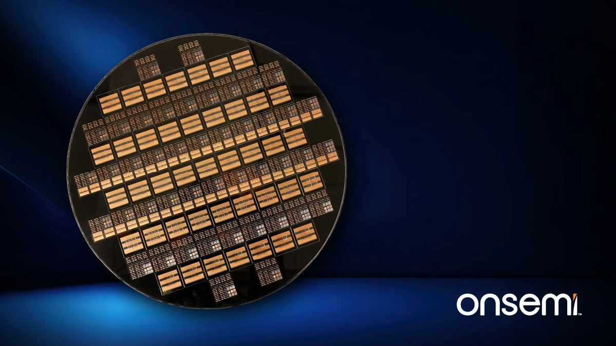
Embedded Power Platform is a new architecture from onsemi, an Arizona chipmaker best known for automotive and industrial silicon, that treats the silicon wafer as the structural base of a module, rather than a separate mechanical shell bolted on afterward. The company claims the approach can lift power density three to five times over current designs, aimed at electricity-hungry AI data centers, electric vehicles, and other demanding systems.
The idea is architectural, not chemical. Rather than housing separate chips inside a passive plastic or ceramic case, EPP folds electrical, thermal, and mechanical engineering into one wafer-level structure from the outset. Silicon, SiC, and GaN devices, including field-effect transistors (FETs), drivers, and controllers, sit together in a single package and get tuned as a unit instead of stitched together after the fact. The design runs on onsemi's existing 12-inch fabrication lines, which the company frames as a route to volume without building new factories.
CEO Hassane El-Khoury pitched EPP as a systems-thinking exercise: pulling process chemistry, packaging, and factory floor into a shared roadmap rather than treating each as a separate handoff, with an eye on AI infrastructure, electrification, and automation.
Subaru Corporation is among the first outside partners the company named for the effort, testing whether EPP suits future electrified-vehicle work; the arrangement gives Subaru early samples, simulation models, and technical support ahead of any broader rollout.
The sales pitch splits by market. AI racks increasingly hand over floor space and cooling budget to power delivery rather than compute; an early EPP-based solid-state circuit breaker came in roughly half the size and about 20 percent cooler than existing designs, the company says, freeing up rack room for more compute in principle. For EV traction inverters, the company cites up to four times the density and roughly 15 percent lower losses versus conventional approaches, plus a single scalable inverter meant to span entry-level to flagship vehicles. Development cycles can shrink to as little as four months, the company says, though none of these figures have been checked by outside labs or tied to a shipping part yet.
The bet is less about beating rivals on raw switching speed than about closing the gap between a lab demo and something a customer can actually order. Packaging has traditionally been an afterthought bolted onto finished chips late in a product's life; folding it into the same roadmap as the transistor itself is a manufacturing-process argument as much as a performance one, and whether it shortens the company's path to real orders from AI hyperscalers and automakers, rather than just its own internal comparisons, will hinge on customers validating results nobody outside the company has yet reproduced independently. Rival chipmakers, from Infineon to Wolfspeed, face the same problem of squeezing more watts into the same rack footprint, so this looks as much like a race to win buyers' trust as a race to finish the part.